
 Electronics Design & Development
 PCB Design & Layout Services
 PCB Fabrication & Prototyping
 PCB Assembly & PCBA Services
Electronics Design & Development
Custom electronics design services, hardware design services and electronics product development support, including schematic design, component selection, prototype bring-up and verification.


Define schematic, PCB layout and manufacturing requirements around project goals.

Agree on source files, review milestones and acceptance criteria before engineering work starts.

Coordinate electronics design, PCB layout, fabrication and assembly as the project requires.

Custom electronics design services, hardware design services and electronics product development support, including schematic design, component selection, prototype bring-up and verification.

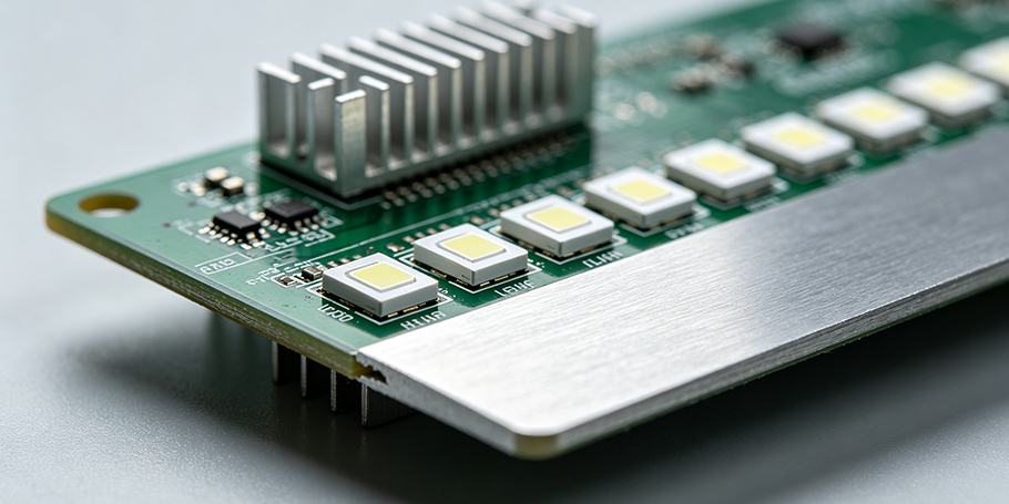
PCB layout services and PCB design outsourcing for high-speed, multilayer, HDI, RF and mixed-signal boards, with stackup planning, engineering review and production-ready design files.

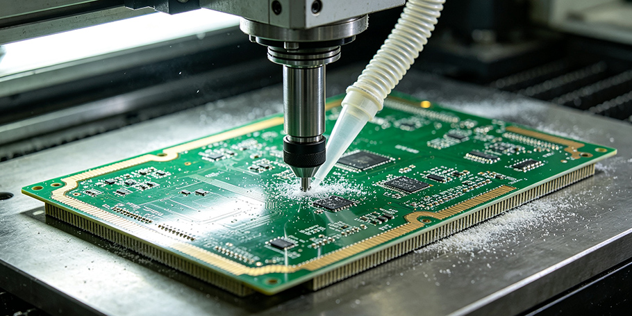
PCB fabrication services and PCB prototyping for multilayer, HDI and high-frequency projects, with board specifications, CAM checks and manufacturing feasibility reviewed before production.

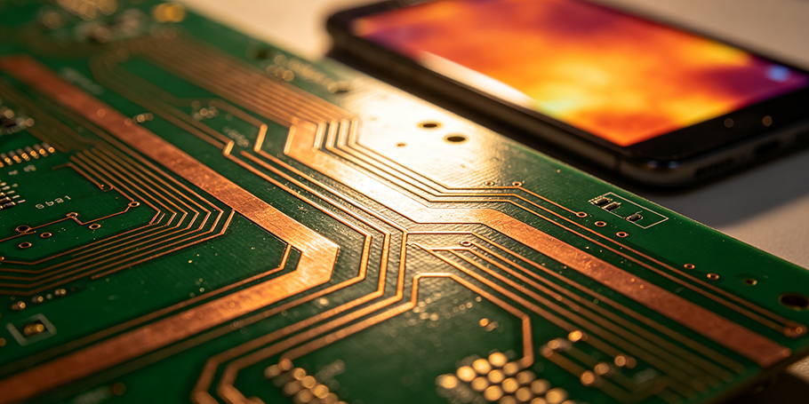
PCB assembly services including SMT PCB assembly, turnkey PCB assembly, prototype PCBA and component sourcing, with inspection and functional testing agreed for each build.
From an initial project brief to an agreed engineering or manufacturing scope, each step clarifies deliverables, review milestones and responsibilities.
Send a functional brief, CAD files or manufacturing data and outline the target schedule.
Review feasibility, critical interfaces, board constraints, BOM or manufacturing questions.
Agree on work packages, file formats, confidentiality terms, acceptance criteria and timeline.
Complete the agreed design or build and review the specified files, inspections or test results.


FYPCB supports global engineering teams with custom electronics design, hardware development, PCB layout outsourcing, PCB fabrication and PCBA services. We review application requirements, design files and delivery expectations with customers, whether the engagement covers a single engineering task or several stages of development and production.

Yes. Custom electronics development, schematic design and PCB layout can be scoped separately. Confirm source-file deliverables and responsibilities in the proposal.
Provide a schematic or netlist, board outline, expected layer count, critical signal constraints and preferred EDA tool where available.
PCB fabrication normally starts with Gerber or ODB++, dimensions and quantity. PCBA also needs a BOM, placement/CPL files and any programming or test instructions.
Raise NDA and secure-transfer requirements in the first enquiry. File access, ownership and confidentiality terms should be confirmed in writing.
Evaluate industrial controller hardware design services by power architecture, field I/O protection, communication, EMC planning, prototype debug and production handover.
view detailsCompare prototype PCBA costs for turnkey and consigned assembly, including stencil, BOM sourcing, SMT setup, X-ray, AOI and functional test.
view detailsPrepare an HDI PCB fabrication RFQ with layer build-up, laser microvias, via-in-pad, stackup, DFM limits and inspection requirements.
view detailsCompare electronics design companies in China by engineering scope, prototype support, deliverables, communication and manufacturing handoff.
view detailsFive circuit schematic problems that pass review and fail on the bench, from collapsing rails and stalled oscillators to reversed connectors and analog drift.
view detailsSix Altium Designer checks we run before releasing a board, from footprint verification and power tree naming to rules, output jobs and variant control.
view details Project-Based Quotation
Pricing follows the agreed engineering or production scope.
 Confidentiality Discussion
Discuss NDA and secure design-file exchange before handoff.
 Delivery Planning
Confirm project milestones and shipping needs at quotation.
 Quality & Review Scope
Define inspection, testing and acceptance requirements by project.


