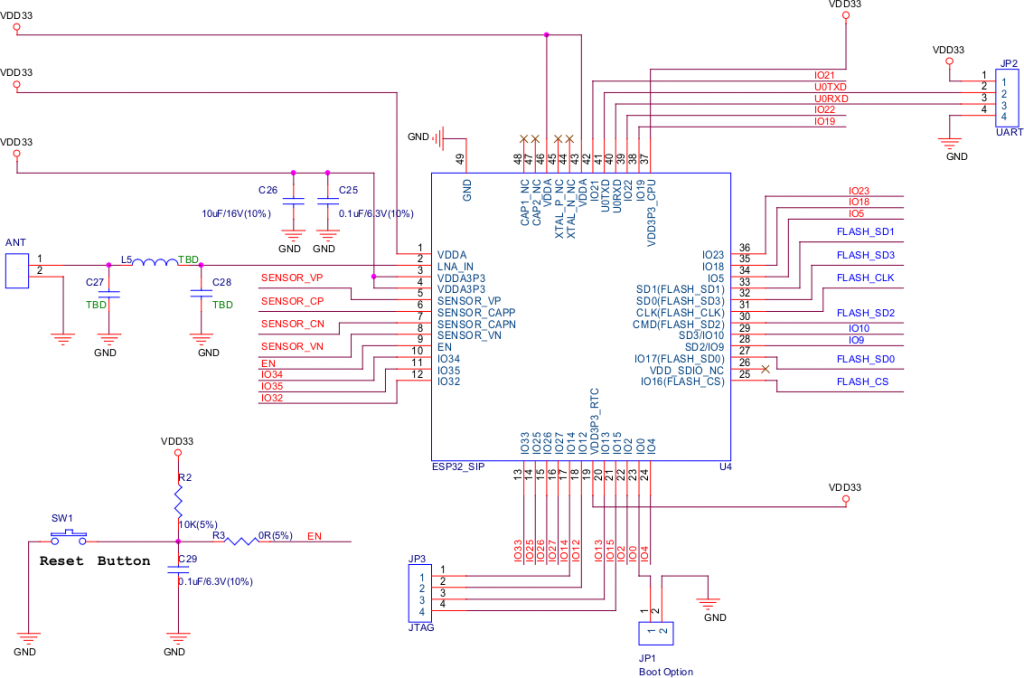
The PCB layout design schematic can be completed in seven steps.
1.Design drawing size
After Open Protel 99/ Schematic, it is indispensable to conceptual parts drawings, set the appropriate size of the drawing, the suitable drawing is based on the scale of the circuit diagram, the appropriate drawing size is the basis for designing schematics.
2.Setting up the Protel 99/Schematic design environment
The environment design mentioned here includes setting the grid size and type, cursor type, etc. Of course, most of the parameters use the default value.
3.Rotating parts
According to the needs of the circuit diagram, the user removes the parts from the parts library and places them on the drawing, and defines and sets the part number and part package of the placed parts.
4.Schematic wiring
With the various tools provided by Protel 99/Schematic, the components on the drawing are connected by electrically conductive wires and symbols to form a complete schematic.
5.Adjusting the circuit line
The preliminary drawing of the circuit diagram is further adjusted and modified to make the schematic diagram more beautiful.
6.Report output
Various reports are generated by Protel 99/Schematic with various reporting tools provided. The most important report is the network table, which is prepared for subsequent board design through the network table.
7.File saving and printout
The final steps are file saving and printout.
if you want to ask some question,you can send email pcb@fany-eda.com.

